Education — Engineering
SolidState
Building semiconductor devices in holographic 3D — layer by layer
Client: CWRU Electrical Engineering / VA Medical Center / IC Fellows Cohort
Challenge
Semiconductor fabrication is an inherently three-dimensional process — layering and removing materials that conduct or inhibit electrical flow. But students learn it from 2D circuit maps and cross-sectional diagrams, struggling to build the spatial intuition needed to design and troubleshoot real devices.
Solution
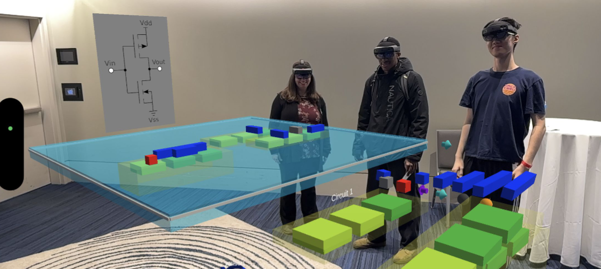
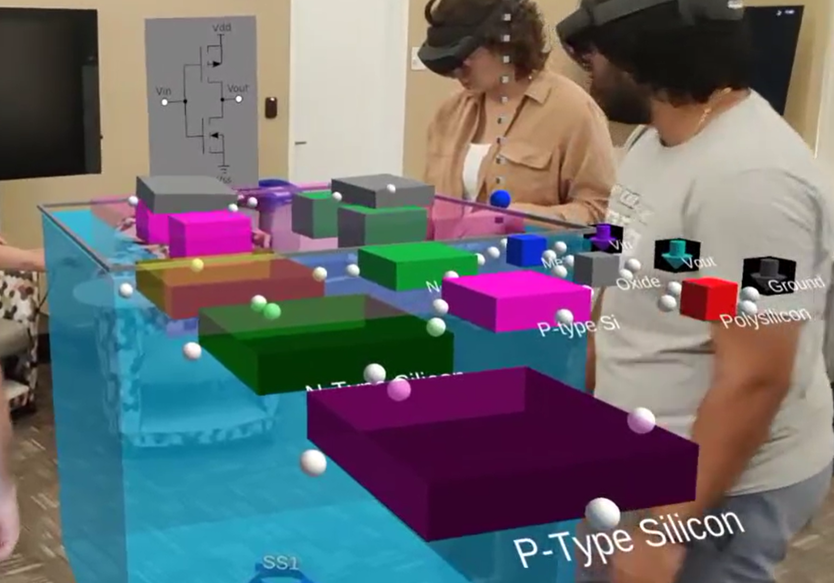
SolidState presents a class of students with the same holographic silicon substrate in a shared 3D environment, alongside a repository of semiconductor components — n-type wells, p-type wells, oxide layers, metal contacts. Following circuit maps, students physically build semiconductor devices together, placing components at precise layers and locations while the instructor guides the group. The hands-on, collaborative assembly builds spatial understanding that diagrams cannot provide.
Results
- •Students physically construct semiconductor devices in holographic 3D
- •Bridges the gap between 2D circuit maps and real fabrication processes
- •Repository of standard semiconductor components for interactive assembly
- •Designed for electrical engineering and biomedical device curricula
- •Developed through CWRU's Provost-sponsored IC Fellows program
The Challenge: Learning 3D Processes from 2D Diagrams
Semiconductor fabrication is one of the most consequential manufacturing processes in the modern world — every chip in every device depends on it. The process is fundamentally three-dimensional: thin films are deposited, patterned, etched, and stacked in precise sequences to create transistors, sensors, and circuits.
But students learn this process from flat diagrams. Circuit maps show top-down views. Cross-sections show one slice at a time. Dr. Allison Hess-Dunning, who teaches semiconductor fabrication at CWRU and conducts MEMS research at the VA Medical Center, saw her students struggling to connect these 2D representations to the physical reality of layered, three-dimensional devices. The mental leap from diagram to device was too large — and too important — to leave to imagination alone.
The Solution: Holographic Fabrication
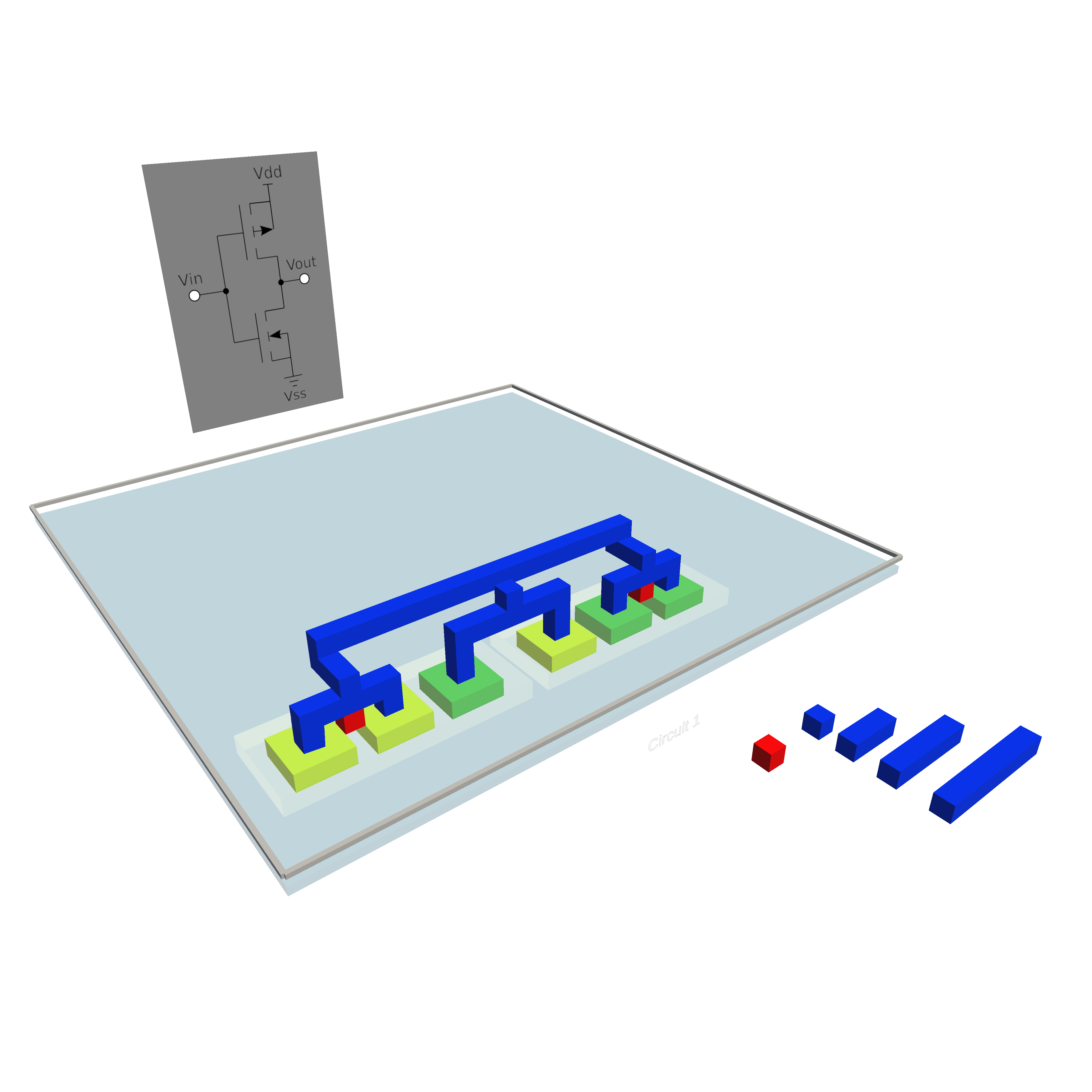
SolidState puts a holographic silicon substrate in front of the student — a bulk wafer they can examine from any angle. Alongside it, a repository of standard semiconductor components: n-type and p-type wells, oxide layers, polysilicon gates, metal contacts, and more.
Following a circuit map, students build semiconductor devices by physically placing components at specific layers and locations on the substrate. They position an n-type well, layer an oxide on top, align a gate — experiencing the fabrication sequence as a spatial, hands-on process rather than an abstract diagram.
The immediate feedback is powerful. When a component is misplaced, students can see the error in three dimensions — understand why a particular layer must come before another, why alignment matters, why the process sequence isn't arbitrary. The device takes shape under their hands, and with it, their intuition for how these structures actually work.
The Impact: From Classroom to Cleanroom to AI-Guided Manufacturing
SolidState bridges the gap between textbook learning and cleanroom practice. Students who have built devices holographically arrive at the fabrication lab with spatial intuition that previously took months to develop. They understand the why behind each process step because they've experienced the consequences of sequence and placement firsthand.
Dr. Hess-Dunning's roadmap extends to additional transistor architectures, MEMS devices, and simulated current flow testing — turning the platform into a comprehensive semiconductor education environment.
The industrial implications are profound. The same approach that teaches students to build semiconductors can train technicians to assemble, inspect, and troubleshoot real devices on the manufacturing floor. With CrewXR's AI integration, organizations can build an intelligent guide: an AI agent that understands the device architecture, watches the assembly process, flags errors before they propagate, and explains not just what to do next, but why — turning every workstation into a master class in semiconductor fabrication.
“Traditional 2D circuit maps and cross-sections prove challenging for students new to the field. They need to see and build these devices in three dimensions.”